Need to measure EUV Photomasks?
We’re here to help.
SHARP is a highly-flexible mask-imaging microscope, staffed by experts in the field, boasting the world’s highest EUV resolution, and designed to investigate the most pressing issues in photomask development and commercialization, now and far into the future.
SHARP (the SHARP High-NA Actinic Reticle review Project) reproduces lithographic imaging conditions (wavelength, NA, and illumination angular spectrum) of all existing EUV lithography tools, and those still on the drawing board.
In recent months, mask development has progressed rapidly and branched in new directions. SHARP’s users target essential and emerging mask issues, using SHARP to answer basic questions, to gather statistics, to test new processes, materials, and architectures, and to look deeply into the future of EUV masks and lithography.
SHARP at a glance
| wavelength = | 13.2–13.7 nm ± 1/1450 Δλ/λ |
| 4xNA = | {0.25, 0.33, 0.4, 0.50, 0.625} |
| CRA = | 6° (typical); 8°, 10° for NA > 0.33 |
| sigma = | 0.05–1+, fully programmable |
| t = | 5–8 sec/image (typical) |
Illumination
SHARP’s lossless Fourier synthesis illuminator provides complete coherence control and engineering to reproduce arbitrary and complex illumination conditions.
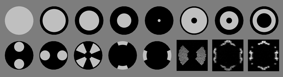
Pupil-Fill Illumination patterns used in SHARP
Sample requirements.
 SHARP can image any 6-inch EUV mask, across the entire front surface.
 Mask navigation can be done either manually (by eye) from a known map, or using fiducial markers and known coordinates for points of interest.
 SHARP can image patterned or reflective blank masks.
 SHARP can accept "wafer-mask" samples, in which a specially prepared, ML-coated, wafer, or wafer piece is attached to a standard 6-inch mask.
 SHARP can measure diced mask pieces if a suitable mask-sized holder were made or provided.
SHARP Mask research issues
| Defects: | native & programmed defects, pattern defects, ML blank defects, phase defects, absorber defects, covered defects |
| Repair Strategies: | imaging before/after repair, through-focus, and under various illumination conditions |
| Mask Architecture and Materials: | line contrast, pattern roughness, exposure latitude, NILS, Bossung plots |
| OPC and Assist Features: | depth of focus, illumination dependence, CD variation |
| ML Roughness: | effect on pattern roughness |
| High-NA effects: | pitch-dependent pattern shift through focus, anamorphic imaging (coming soon) |
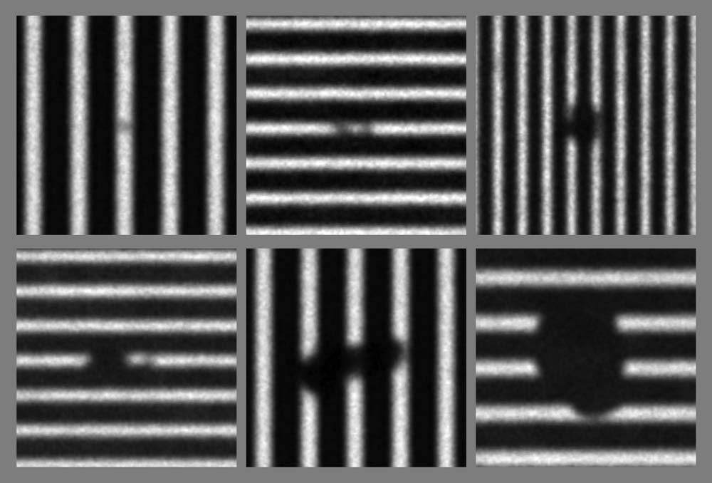
Various native defects imaged with SHARP
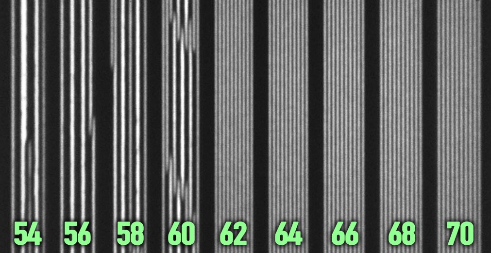
SHARP images of a resolution test mask. The line-width half-pitch values are shown in nm. This mask suffers from "pattern collapse" for features below 62 nm.
Advanced optical techniques used to extract more information from masks and now under development.
| Phase Imaging: | for understanding roughness and repair; through-focus phase reconstruction; Fourier-ptychography microscopy (FPM); differential phase contrast (DPC); Zernike phase contrast (ZPC) |
| Anamorphic Imaging: | emulating future litho tools with different x and y NA and magnification |
| High-Angle Multilayer Development: | performance of EUVL at central ray angles beyond 6°, with 4xNA values above 0.35 |
| Source-Mask Optimization (SMO): | customizing source pupil fill and mask patterns for improved imaging metrics |