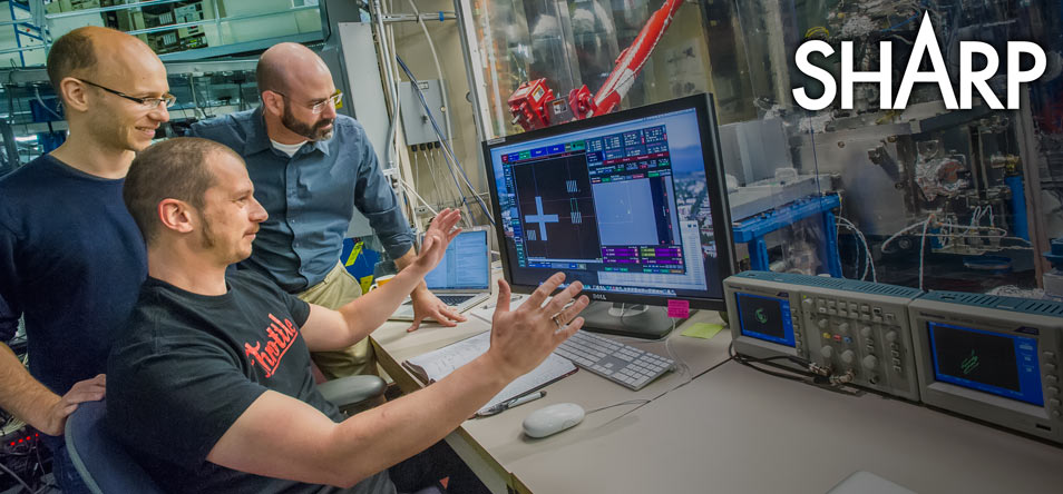
SHARP is a powerful tool for Extreme Ultraviolet (EUV) Lithography and photomask research, and one of the most advanced short-wavelength microscopes ever created. Funded initially through SEMATECH, and supported by visionary leaders at leading semiconductor companies, SHARP was created by the Center for X-Ray Optics (CXRO) at Lawrence Berkeley National Laboratory (LBNL). It operates on a synchrotron bending-magnet beamline at the Advanced Light Source (ALS).
 The need for, the requirement for actinic (i.e. EUV wavelength) inspection of photomasks was firmly established years ago. The earliest experiments in actinic mask inspection confirmed the wavelength-specific response of multilayer, surface, and “buried” substrate defects, and revealed a long-theorized category of so called phase-defects, which largely evade detection by other means.
Numerous experiments conducted on the Actinic Inspection Tool (AIT), SHARP’s predecessor at LBNL, showed the inconsistent interplay of deep ultraviolet (DUV), scanning electron microscope (SEM), atomic-force microscopy (AFM), and EUV imaging of native and programmed defects. This situation arises from the fact that photomasks—consisting of a glass substrate, a multilayer coating, capping and buffer laters, and patterned absorber materials—are inherently complex optical systems pushed to their extreme limits to produce optimal pattern transfer into photoresist. All of the materials, and the details of their combination, show a vastly different physical response to probes of different kinds. For example, AFM sees only the top-surface contour, where bumps and pits might be detectable. While SEM and DUV inspection modes only penetrate the first few nm of the top surface, each in different ways. Subtle surface height relief shows no contrast to these probes. Only EUV light at-wavelength senses the subtle imperfections throughout the mask coating, extending all the way through the structure, revealing the conditions most relevant to lithographic printing. Making matters more complex is the fact that defect severity can change with varying illumination conditions.
 Among available tools for studying defects and their response, the SHARP microscope uniquely reproduces the correct wavelength and illumination conditions in any current or future EUV lithography tool, out to 4xNA values of 0.625, and off-axis angles of incidence up to 19°, should EUVL move in that direction. Whether the future brings higher mask-side NA values, higher magnification, anamorphic imaging, source-mask optimization, or any combination of these, SHARP is ready to provide real-world aerial imaging to guide the strategic decision-making.
 While SHARP is well suited for studies made with current EUV lithography conditions, SHARP will really shine studying future directions in EUVL—the kinds of real experiments that are nearly impossible to conduct in other ways. Whether it’s detailed tests of novel illumination pupil-fill patterns, emerging defect repair or covering methods, exotic high-angle multilayers, or extended-NA or anamorphic imaging, let SHARP light the way forward. Our well-trained team of scientists/operators can help you get the best possible data. Of course, our team strictly respects the privacy and business sensitivity of the work we do and the companies we work with. Nothing about our users’ work is disclosed or shared without permission, and safeguards are in place to securely control access to collected data.